Back to Main Menu
Hardware Design
There are certain steps that we have to take to churn through this phase of the project. This is where we will create the schematics, then layout the PCB and discover the true limits for the size of the project.
The software we use for creating our schematics and laying out the PCB is called KiCad. KiCad is open-source software built by the community. It is by far the best free tool out there for anything PCB.
Schematics
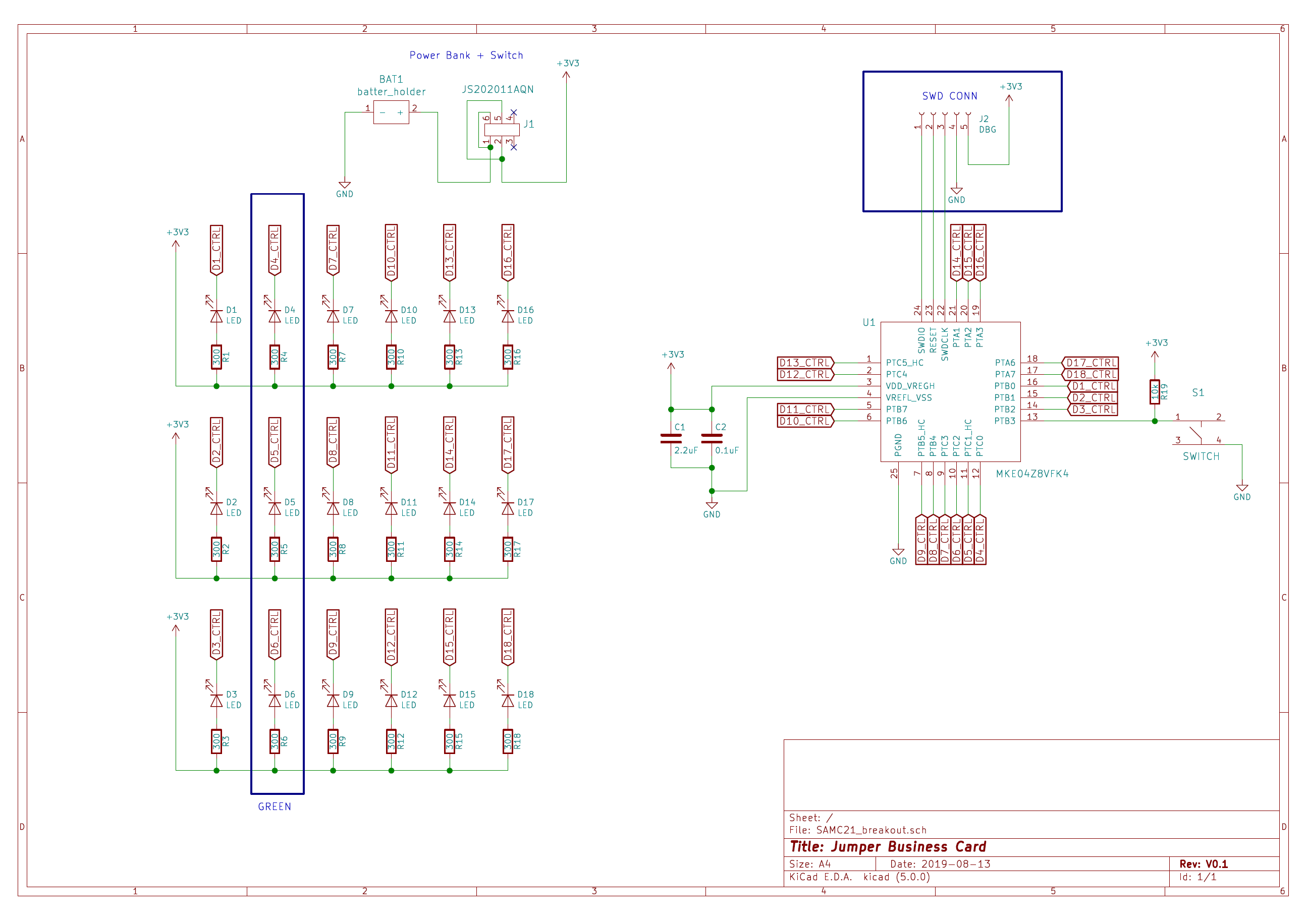
Below
It is very important to note that at this stage we have to think about all the components and how our circuitry will function. One major issue is how we will drive the LEDs. As one guru has once taught me, an MCU can drive very little, but it can sink a lot. This is why all the LEDs are directly connected to the positive terminal of the battery, while the other side is connected to the MCU. This means that when we drive a GPIO high, we will stop the flow of energy and thus turn on the LED and opposite, when we drive the GPIO low, we will turn on the LED. This operation has to be verified with the datasheet to ensure that this operation will not be out of spec.

PCB Layout
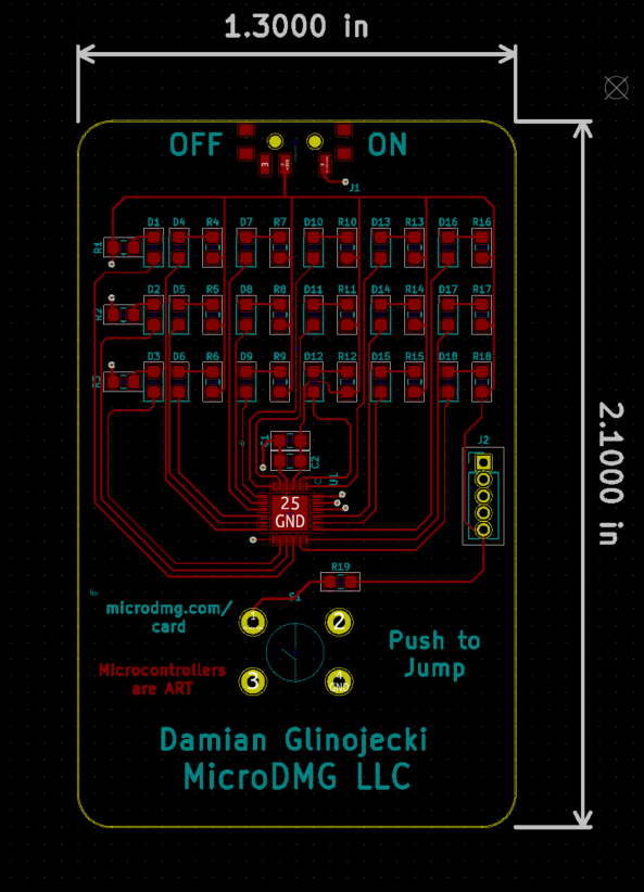
PCB Layout was very important for this project as the PCB would be exposed and it would be the main interaction point. LEDs had to be arranged in a screen like fashion with distances carefully measured, the button had to be easily pressable with a single
The size was a fine balance between cost and functionality. The number of components was not the issue (as usually is), instead, this board could have been made much smaller, but that did not make sense in this case. The board had to be big enough to comfortably fit into the palm of a hand.
Component Placement Strategy
Many think that PCB boards are populated at random, that is definitely not the case. Many hours of careful planning go into this step as it determines how easy your routing will be. Some of the components are often locked into place by the fact that they have to be in a certain position. In this case, the LEDs and the button were predefined and everything else had to be worked around these components.
There are also components that need to be physically close to other components. This is especially true for the decoupling capacitors. You need to place decoupling capacitors as close to the component that it will be

Once all the components are placed, it is time to route. I usually start routing while placing the components to see where I physically need more space to route with as little vias as possible. Once all my placing and routing is done, you cannot forget about silk screen. All components are neatly labeled, necessary information is placed and then decorative labeling, logos and so forth is included.
KiCad includes logic for making sure that no connection is left out. This is very useful as it is easy to omit something, especially when the project gets very large. When everything looks good, it is time to export the Gerber files and
Part 3: Firmware Walkthrough